Driver Assistance: Protecting adas
Tony Armstrong from Analog Devices discusses why automotive adas need low EMI and EMC emission switching converters
The adas market is expected to reach $60bn globally by 2020, according to Allied Market Research. This represents a CAGR of 22.8% from 2014 to 2020. Clearly, this is a significant opportunity for semiconductor content.
Adas is an acronym for advanced driver assistance systems commonly found in many of today’s new automobiles. These usually facilitate safe driving and can provide the driver with an alert if the system detects risks from surrounding objects such as errant pedestrians, cyclists or even other vehicles on an unsafe trajectory.
Furthermore, they typically provide dynamic features such as adaptive cruise control, blind spot detection, lane departure warning, driver drowsiness monitoring, automatic braking, traction control and night vision. As a result, it is the increasing focus of consumers on safety, demands for comfort while driving and the continued increase of government safety regulations that are main growth drivers of adas in automobiles for the latter half of this decade.
This growth does not come without challenges for the industry, which include pricing pressure, inflation, complexity and difficulty in testing. Moreover, it should come as no surprise that the European automotive industry is one most innovative automotive market and, as such, it has seen major market penetration and adoption of adas from its customers.
Nevertheless, both the American and Japanese car makers are not far behind. The ultimate goal is an autonomous driving machine without the need for a human being behind the wheel.
Challenges
Generally speaking, adas incorporate some kind of microprocessor to gather all the input from the numerous sensors within the vehicle and then process them so that they can be presented to the driver in a way that can be easily understood. Moreover, these systems are usually powered directly from the vehicle’s main battery that is a nominal 9 to 18V, but could be as high as 42V due to voltage transients within the system, and as low as 3.5V during a cold-crank condition. Thus, it is clear that any DC-DC converters within these systems must be able to handle the wide input voltage range of 3.5 to 42V, at a minimum.
Many adas use a 5 and 3.3V rail to power their various analogue and digital IC content; however, the processor IO and core voltages that are typically used will have operating requirements in the sub-2V realm, and could be as low as 0.8V. Furthermore, the system is usually mounted in a part of the vehicle that is both space and thermally constrained, thereby limiting the heat sinking available for cooling purposes.
While it is commonplace to use a high voltage DC-DC converter to generate a 5 and 3.3V rail directly from the battery, in today’s adas a switching regulator must also switch at 2MHz, or greater, rather than the historical switching frequency of sub-500kHz. The key driving force behind this change is the need for smaller footprints while also staying above the AM frequency band to avoid any potential interference.
Finally, as if the designer’s task is not already complicated enough, they must also ensure that the adas comply with the various noise immunity standards within the vehicles. In an automotive environment, switching regulators are replacing linear regulators in areas where low heat dissipation and efficiency are valued.
Moreover, the switching regulator is typically the first active component on the input power bus line, and therefore has a significant impact on the EMI performance of the complete converter circuit.
There are two types of EMI emissions; conducted and radiated. Conducted emissions ride on the wires and traces that connect up to a product. Since the noise is localised to a specific terminal or connector in the design, compliance with conducted emissions requirements can often be assured relatively early in the development process with a good layout or filter design.
However, radiated emissions are another story altogether. Everything on the board that carries current radiates an electromagnetic field. Every trace on the board is an antenna and every copper plane is a resonator. Anything other than a pure sine wave or DC voltage generates noise all over the signal spectrum. Even with careful design, a power supply designer never really knows how bad the radiated emissions are going to be until the system gets tested. And radiated emissions testing cannot be formally performed until the design is essentially complete.
Filters are often used to reduce EMI by attenuating the strength at a certain frequency or over a range of frequencies. A portion of this energy that travels through space (radiated) is attenuated by adding metallic and magnetic shields. The part that rides on PCB traces (conducted) is tamed by adding ferrite beads and other filters. EMI cannot be eliminated but can be attenuated to a level that is acceptable by other communications and digital components. Moreover, several regulatory bodies enforce standards to ensure compliance.
Modern input filter components in surface-mount technology have better performance than through-hole parts. However, this improvement is outpaced by the increase in operating switching frequencies of switching regulators. Higher efficiency, low minimum on- and off-times result in higher harmonic content due to the faster switch transitions. For every doubling in switching frequency, the EMI becomes 6dB worse while all other parameters, such as switch capacity and transition times, remain constant. The wideband EMI behaves like a first order high pass with 20dB higher emissions if the switching frequency increases by ten times.
Savvy PCB designers will make the hot loops small and use shielding ground layers as close to the active layer as possible. Nevertheless, device pin-outs, package construction, thermal design requirements and package sizes needed for adequate energy storage in decoupling components dictate a minimum hot loop size. To complicate matters further, in typical planar PCBs, the magnetic or transformer style coupling between traces above 30MHz will diminish all filter efforts since the higher the harmonic frequencies are, the more effective unwanted magnetic coupling becomes.
Dual converter
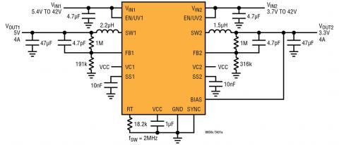
The application constraints described led to the development of high input voltage capable, dual output monolithic synchronous buck converters, such as shown in the diagram, that also have low EMI and EMC emissions. The 3 to 42V input voltage range makes it suitable for automotive applications, including adas, which must regulate through cold-crank and stop-start scenarios with input voltages as low as 3V and load dump transients in excess of 40V.
As can be seen in the diagram, this dual channel design consists of two high voltage 4A channels, delivering voltages as low as 0.8V, enabling it to drive the lowest voltage microprocessor cores available. Its synchronous rectification topology delivers up to 94.4% efficiency at a switching frequency of 2MHz, while burst mode operation keeps quiescent current under 6.2µA (both channels on) in no-load standby conditions, making it suitable for always-on systems.
The switching frequency can be programmed from 300kHz to 3MHz and synchronised throughout this range. Its 40ns minimum on-time enables 16Vin to 2.0Vout step-down conversions on the high voltage channels with a 2MHz switching frequency. Its architecture uses two internal input capacitors as well as internal BST and INTVCC capacitors to reduce the area of the hot loops.
Combined with well controlled switching edges and an internal construction with an integral ground plane and the use of copper pillars in lieu of bond wires, the design reduces EMI and EMC emissions.
This improved EMI and EMC performance is not sensitive to board layout, simplifying design and reducing risk even when using two layer PCBs. It can easily pass the automotive Cispr 25, class five peak EMI limits with a 2MHz switching frequency over its entire load range. Spread spectrum frequency modulation can lower EMI levels further.
The internal top and bottom power switches with the necessary boost diode, oscillator, control and logic circuitry can be integrated into a single die. Low ripple burst mode operation maintains efficiency at low output currents while keeping output ripple below 10mV p-p. This can all fit into a thermally enhanced 4 by 6mm 32-pin LGA package.
Conclusion
There can be no doubt that the proliferation of adas in automobiles is not going to end anytime soon. Furthermore, it is also clear that finding a power conversion device that meets all the necessary performance metrics so as not to interfere with the adas is not a simple task. Fortunately for the designers of these systems there are now power converters that simplify their task while simultaneously delivering the performance they need without requiring sophisticated layout or design techniques.
Tony Armstrong is director of product marketing for the power products group at Analog Devices