Simulation & Modelling: Keeping balance
Jon Munson of Linear Technology explains how to build an electronic battery simulator
Many new products are incorporating lithium-based batteries for the high performance and light weight characteristics they offer. Prime examples include the newest crop of all-electric vehicles and hybrid electric vehicles coming out of Germany, such as BMW’s i3 and i8, and VW’s Passat. All these, as well as more sophisticated applications, involve connecting a multitude of cells to achieve the desired pack working voltage, often hundreds of volts.
Since lithium cells are prone to ill effects if allowed to over charge or over discharge, these series packs incorporate monitoring systems that keep tabs on each cell potential to avoid such problems. The process of developing such a multi-cell battery monitoring system (BMS) requires a convenient means of stimulating the circuitry to test the effectiveness of the control and protection algorithms.
Ideally, the stimulus would be actual cells, but then to vary the state-of-charge (SoC) to trigger different functional actions in the BMS becomes a slow and cumbersome matter. Multiple lab power supplies are frequently used but this is very expensive. So for simple functional tests, resistor strings are often just biased to provide a rudimentary cell simulation.
The resistor strings have significant limitations since they present a fairly high source resistance, and thus introduce system artefacts that are not representative of actual cells. Even with dedicated supplies though, if the system under test involves active cell balancing, then the supplies must accommodate virtual charging current, or current reversal.
The bottom line is that it is desirable to have a means of having a multiplicity of compact cell simulators to provide easy lab testing of the BMS functionality. Another useful aspect of having a battery simulator is that such an item is readily transportable by air freight for operations away from the laboratory, whereas an actual lithium cell pack usually has to be shipped by surface vessel.
Practical circuit
The primary feature that is needed is low source impedance and two-quadrant operation – positive voltage but bidirectional current, so both discharge and charge directions can be simulated. The various cell simulators need to be isolated so they may be wired in series like the actual pack. This latter requirement suggests the use of transformers and, for compactness, a switching-type architecture. One particular switching topology offers both isolation and two-quadrant operation, namely the synchronous flyback converter.
In a simple flyback converter used as a voltage booster, a low-side switch operates at a duty cycle that sets the output current on an output section. In this idealised form, the rectifier diode conducts during the time the switch is off, and allows output current to flow in the inductor as magnetic energy is transferred to the output capacitor in a unidirectional fashion. When regulating, the switch experiences a flyback peak voltage dV above the 12V supply, where dV is of the order of the supply voltage in most designs.
To make the converter isolated, replace the inductor with a transformer so the output appears on the secondary side. While the output is now isolated, the magnetic energy transfer is just the same as an inductor. The transformer turns-ratio N is selected to optimise the operation with the specific input and output voltages desired. Here again, the switch experiences a flyback peak voltage dV above the 12V supply. Notice that this circuit cannot prevent the output voltage from being forced above the set-point by an external current – this only supports one quadrant of operation.
A synchronous version is created when the rectifier is replaced by another switch. This both improves the efficiency, since the switch will dissipate less power than a forward-conducting diode, and creates a second quadrant of operation because now the circuit has symmetry.
This circuit can accept reverse current in the secondary that induces primary winding flyback current back into the main supply, thus the output will hold its set point even with a forced reversed output current. The designer needs to be cognisant of the possibility that the source supply for the circuit could itself experience a reversed current if the simulated cell is being heavily charged, that is with current flowing into the positive output voltage.
Since the outputs are all isolated, the source power can be shared among any number of circuits so a single bulk supply can conveniently provide power to an entire array. Such an array connection also consolidates the parasitic circuit losses so it becomes unlikely that the source supply experiences a current reversal in normal usage, that is as long as net charging power is less than total operating losses.
Details
The typical application for a suitable circuit is to provide low, battery-like voltages at several amps from higher voltage bulk supply rails. The only difference for the cell simulator function is that an adjustable output voltage could be beneficial. Since turnkey high-power bulk supplies are available at 12V, the design can be optimised to use this as a source.
Given the range of lithium cell chemistries is from just under 2V to just over 4V, a corresponding tuning range can be established that provides versatile usage and the ability to simulate a wide range of SoC states.
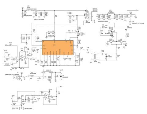
Fig. 4 shows one section of an array with all the part details. To provide voltage adjustment, the feedback network supports an op amp control signal such that zero volts represents about 4.2V output and 3V commands about 1.9V out. For good user control, each cell circuit is configured to have a vernier fine tune, and then an array set is group controlled with a coarse and fine adjust – master adjustment signal MCTL can be connected to several converter sections.
For the values shown, the output voltage group coarse is about ±0.9V, the group fine is about ±0.15V, and the cell verniers are about ±0.1V, so collectively the maximum desired range is achieved; to provide vernier controls, ability to cross-control cells to the full limits was sacrificed. All the control circuitry is powered by 3.3V derived from the 12V bulk supply. For computerised voltage control, the op amp signals can be replaced with DACs.
In the diagram, Q101 and T100 are the main flyback elements, with Q102 being the synchronous rectifier. For fast and isolated control of Q102, the gate is driven by T101 via current buffers Q103 and Q104. Feedback is scaled from an auxiliary winding in T100. A 10mΩ series resistor is included at the output so that current sense measurements are possible by taking Kelvin connections to a voltmeter, by use of signals I+ and I-. The total output impedance of the circuit is about 25mΩ and provides a solid ±6A capability. Static losses are about 1W per cell section, so with an array of 24 cells, the likelihood of a 12V supply reversal is minimal and the power level scales well for use with an off-the-shelf 12V, 300W supply.
Conclusion
It is clear that EVs and HEVs are growing in number and consumers are demanding long life, as well as long run times from the battery packs used inside them. Consequently, a battery simulator is a key tool for understanding how these battery packs will perform once installed within a vehicle. As a result, building battery simulators is a practical way to provide a high density and easily transported BMS development tool. A 24-cell simulator can be packaged in a 2RU rack-mountable chassis complete with a 12V bulk supply, and provide precisely adjustable voltages in the 1.9V to 4.2V range with ±6A capability.
Jon Munson is an applications engineer with Linear Technology