Adapting to adas design flows
Developers of modern advanced driver assistance systems (adas) face a challenge when adopting the latest technology without risking missing their market window, says Stephan Janouch
While there are still many legislative challenges ahead, the dream of autonomous vehicles is a technical reality. As a result, demand for more advanced adas is rising, putting increased pressure on OEMs and tier-one suppliers to make best use of the latest technologies. This can often be a challenge in the automotive domain, due to the relatively long design cycles and overall product lifetimes required. Many integrated devices are evolving too quickly for automotive manufacturers to make full use of them; before they’re fully designed-in they’ve been replaced or upgraded.
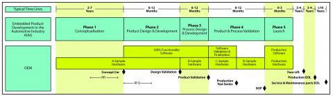
The diagram illustrates the problem, showing that development on the electronic system(s) can start as much as three years before the vehicle is expected to go in to production, with all parts being available more than ten years later.
One solution to this problem is to use asics, but while they offer the security of guaranteed supply, their design is highly specialised and costly, and they remain inherently inflexible and not easily able to adapt to the rapidly evolving world of adas. The alternative would be an ASSP, developed by an integrated device manufacturer (IDM) specifically for the automotive market. These typically comprise a standard microcontroller or DSP architecture, coupled with peripherals designed for automotive applications.
The design effort in this scenario is predominantly in the software running on the ASSP. It has been well documented that electronic design teams now comprise mostly of software engineers; hardware having become almost standardised, it is in the software that OEMs are now able to differentiate most strongly.
Despite understanding their relative benefits, many tier-one suppliers still favour an MCU-DSP approach over the third option of an FPGA. Often this is not because they can’t provide a better method — in fact their flexibility means they are much better suited to applications with rapidly changing requirements (such as adas) — but because of a higher perceived level of complexity at the design stage.
Hardware description languages (HDLs) have long been the standard method of developing asics, as well as designing and configuring FPGAs. Within today’s teams of software engineers, few will have experience or expertise in VHDL or Verilog, and this may be because asic design is often outsourced to a specialist provider. As such, adopting an FPGA in a design flow would require an engineering team with expertise in HDL.
If this impasse were to be removed, OEMs and tier-ones would be free to exploit the potential of FPGAs much more easily. This is even more relevant when developing an adas system.
Visionary
Much of the effort going in to developing adas products is focussed on fusing the input from multiple sensors, to provide enough data for the system(s) to make a decision, such as when to apply the brakes, when to alert the driver or even when to take control of the steering column.
The predominant technology used here involves some form of image capture, be that using radar, ultrasonic sensors or cameras. Bringing all these data together and processing them requires an immense amount of processing power; by using an FPGA a large amount of that processing burden can be accelerated using hardware instantiated in the logic fabric.
Many modern FPGAs now implement high-performance multicore Arm-based processing subsystems, which are closely integrated to the logic fabric. Adas applications can therefore be optimised to run in the processor subsystems, supported by hardware acceleration (such as DSP blocks) that works seamlessly with the embedded software.
FPGA platforms that integrate Arm processor subsystems also provide the perfect environment for integrating existing IP, written and verified in an HDL, to run alongside the application software. Developing such a method incurs much lower NRE than an asic, while remaining much more flexible to future changes.
To give OEMs and tier-ones access to this new class of FPGA, IDMs are making it easier to integrate them in to an existing, software-centric design flow. By using high level synthesis, it is now possible to bypass the HDL stage, removing the need for specialist knowledge of Verilog or VHDL, or even a classic FPGA design flow. Instead, software developers can target these platforms using conventional C/C++.
Without this approach, engineering teams targeting an FPGA would need to translate the C/C++ algorithm to HDL manually; a process that is laborious and error-prone. Using a form of high-level synthesis, the translation from software to hardware – or synthesis – is handled by the development environment, resulting in a combination of hardware and software optimised for the application, generated from just C/C++.
This has far reaching benefits, as not only does it allow development teams to implement a design more effectively, it also offers the ability to optimise a design for performance and/or power consumption. Simpler synthesis means it is easier for engineering teams to target the right platform, as it can be scaled up or down to suit the requirements. Simpler design migration also allows any future features to be accommodated, by moving to a platform with greater performance or capacity in the logic fabric.
Tool for the job
Using an HLS tool for software and hardware co-development when targeting an FPGA featuring, say, an Arm processor sub-system means design optimisation becomes much more specific to a particular device within the family.
When the processors in each member of the family are identical, software development can start much earlier in the design cycle. As the design develops, the design environment can support design partitioning, allowing the implementation to adapt to changing or evolving performance goals, based on the available resources. This flexibility allows the design team greater freedom when selecting the best part for the application. Once developed, the design environment can automatically generate the configuration data from the high-level source code, be that C, C++, System C or Open CL.
The same design flow can be used in FPGAs that don’t have an Arm core sub-system; in this scenario the engineering team would generate hardware IP from algorithms (software) without the need to employ RTL. The design environment can then take that IP and integrate it with existing IP.
Conclusion
While there is much work to be done to make autonomous vehicles a reality, and the legislative process will likely be lengthy, adas systems are developing at a rapid rate. Car manufacturers can’t afford to wait to implement new systems, and consumer demand and expectation is already escalating. Self-parking cars and rear-view cameras are only the beginning; as adas penetrates every aspect of driving, road users and pedestrians can look forward to a much safer environment.
The use of FPGAs will help accelerate the next generation of adas, supported by powerful hardware platforms and more sophisticated software development environments, underpinned by high-level synthesis.
Stephan Janouch is senior manager for automotive marketing in Emea for Xilinx