Infotainment: Power on
Marco Gaeta and Carlo Protti from ST Microelectronics explain how an integrated power management IC can benefit automotive infotainment application
Many infotainment and dashboard systems require the battery voltage to be distributed and converted to a lower voltage. Automotive step-down or buck regulators provide this function.
Regulators directly connected to the vehicle battery, used as pre-regulators, conduct different functions. At first, they protect the supplied application from battery fluctuations – transient supply voltages caused by load dump, for instance – thereby avoiding an addition of expensive countermeasures at the application side. Then, they are capable of converting the typically 5 to 15V battery voltage source into a lower regulated voltage, typically 3.3 to 10V.
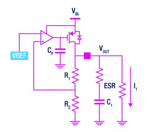
Linear regulators use a resistive voltage drop to regulate the output voltage, dissipating power in the form of heat. They provide a very stable voltage, with low noise and high bandwidth, at the cost of higher power dissipation, depending on the voltage difference between the input and the output. The package itself can have problems when it has to manage high power.
Looking at the diagram:
PdissLDO = (Vin-Vout) * Iout
Switching regulators work with a phase difference of 90˚ between voltage and current and are much more efficient than a linear regulator. Less energy is lost, thermal management becomes easier, and smaller components can be used. On the other hand, switching regulators can be noisy and require a control loop to manage the energy, and often switches (mos) are external, increasing the BoM list.
By defining the efficiency (E) of a switching regulator as the ratio between output and input power:
E = Pout/Pin = (Vout * Iout)/(Vin * Iin)
The power dissipation is given by:
PdissSW = Pin-Pout = (1-E)*Pin
A complex power management system requires a large number of ICs: pre-regulators and post-regulators with different output voltages and current requirements, mosfets, and many others. Design engineers can consider using a single integrated product that embeds switching mosfets, which can be used for pre-regulation when connected to the vehicle battery, or for post-regulation when connected to a lower voltage. This, in addition to decreasing time to market, provides the ability to add features that can simplify the design, application size and cost.
A single package with more than one regulated output voltage and independent supply pins can help increase the efficiency of the system if one of the outputs is used as pre-regulator and the remaining outputs as post-regulated voltage, having their supply connected to a voltage lower than the battery, provided by the pre-regulator. The flexibility offered by such compactness can be enhanced by added features that don’t need to be provided by other external ICs.
When the power stage is done by internal switches in high and low side configuration, their size can be optimised to reduce the on-resistance and therefore the conduction losses. The conduction power loss (Pcon) is directly proportional to the square of the average current in the power (Irms) and the on-resistance (RDSon) of the power itself.
Pcon = I2rms * RDSon
Switching and gate driver losses can be reduced with an optimised design of the driving stage of internal switches. Knowing the switching mosfets in an integrated IC, this operation is simplified.
The high and low side charging and discharging phase is very important from a timing point of view, together with the dead time between the high side turning off and low side turning on phase: all these phases directly affect the entire regulator efficiency in terms of gate driver losses and switching losses.
Gate driver losses are given by:
Pdriver = PgateHS + PgateLS = (QGHS+QGLS) * Vdriver * Fsw
The losses are directly proportional to the charge to be provided to the power gate, the driving stage supply voltage, and the switching frequency (Fsw).
Switching losses (Psw) are related to internal switch turning on-off time (trise and tfall) and are given by the formula:
Psw = 0.5 * Vin * Iload * Fsw * (trise + tfall)
It even depends on the regulator load current (Iload), switching frequency (Fsw), and the input voltage at the power stage (Vin).
The last parameter to be considered is the dead time, which is very important for avoiding high and low side cross conduction that can lead to a broken power stage. During this time both the switches are off so the inductor current is flowing through the power parasitic body diode, adding to the losses due to the diode voltage drop – higher than the drop on the turned on power switch.
The efficiency of the buck converter heavily depends on all these contributions, and leaving their selection to the engineering team could just add more risk; they already have to deal with external components and PCB traces losses.
Power good signals, used to highlight that the output voltage has reached the correct value, together with input and output voltage monitors, thermal and over current protections, could be freely available in a more robust integrated product.
Integrating more switching regulators in the same package can cause noise problems, so managing EMI could be one of the issues affecting the application’s performance. An easy countermeasure is to work with different phases: for instance, two DC-DCs can work with a 180˚ phase shift and reduce emissions. Also important for EMI management is the driving stage: the faster the stage, the higher the noise, even if efficiency is improved. For an exact design, the right trade-off between EMI and efficiency should be found.
When more than one IC is used, if they work at the same or multiple switching frequency, their operation can be guaranteed stable. The device should be able to synchronise to an external signal and send a synchronising signal.
Another issue to be dealt with when switching voltage regulators are used, especially important in a car when the IC has to work near a tuner, is AM band interference. The switching frequency should be higher than the maximum frequency content of this band – higher than 1.7MHz. This can be accomplished with an internal oscillator able to work at high frequency, or with a synchronising pin where the engineer can use a desired frequency. A higher frequency also helps reduce the size of the external inductors.
Modulation control methods used in buck regulators often include voltage mode (VM) and current mode (CM) controls. Current mode control makes it easy to compensate loop and line feed-forward. Voltage mode control is usually less noise sensitive.
Both methods present advantages and disadvantages, but they are not the main worries when designing a power supply.
The switching regulator requires the correct sizing of output inductor and capacitor and input capacitor.
The correct sizing of the output inductor makes it the most difficult to design. Usually it works in continuous conduction mode (CCM). The inductor does not fully discharge during the switch-off time, and its current is always positive. In discontinuous mode, the current goes to zero and can impact EMI, so avoiding this condition is preferred. The load current threshold between continuous and discontinuous modes is given by:
IloadminCCM = [(1-D)*Vout]/(2*L*Fsw)
The threshold depends on switching duty cycle (D = ton/Tsw), output voltage (Vout), the switching frequency and inductor value: the bigger the inductor, the lower the threshold when entering continuous current mode, but at the price of higher cost and larger footprint on the PCB.
Besides, a bigger inductor is useful for reducing the current ripple (∆IL), transformed into a voltage ripple (∆Vout) at the regulator output by the output capacitor parasitic resistance (ESR) as first approximation:
∆Vout = ESR*∆IL
The ESR can be reduced by using a higher quality capacitor or by putting several capacitors in parallel. In addition, the output capacitor reduces the voltage overshoot of the regulated voltage during dynamic load transient and directly contributes to loop stability.
∆Vout = L/2*(I2loadmax - I2loadmin/(Cout * Vout)
The noise and the ripple at the input of the power supply is reduced acting on the input capacitor, which has to withstand the maximum input operating voltage and the maximum RMS input current required by the device. The input capacitor must deliver the RMS current according to the equations below depending on the duty cycle D:
IRMS = Iloadmax * √[D*(1-D)]
Quiescent current and efficiency are two important parameters to consider when dealing with automotive parts. The vehicle battery should not discharge when the on-board electronics are put in stand-by. The IC should not reach a high temperature and should not require a cooling system to reduce system costs and guarantee reliability.
Marco Gaeta and Carlo Protti work for ST Microelectronics